Novena iCE40 Add-On Part 3

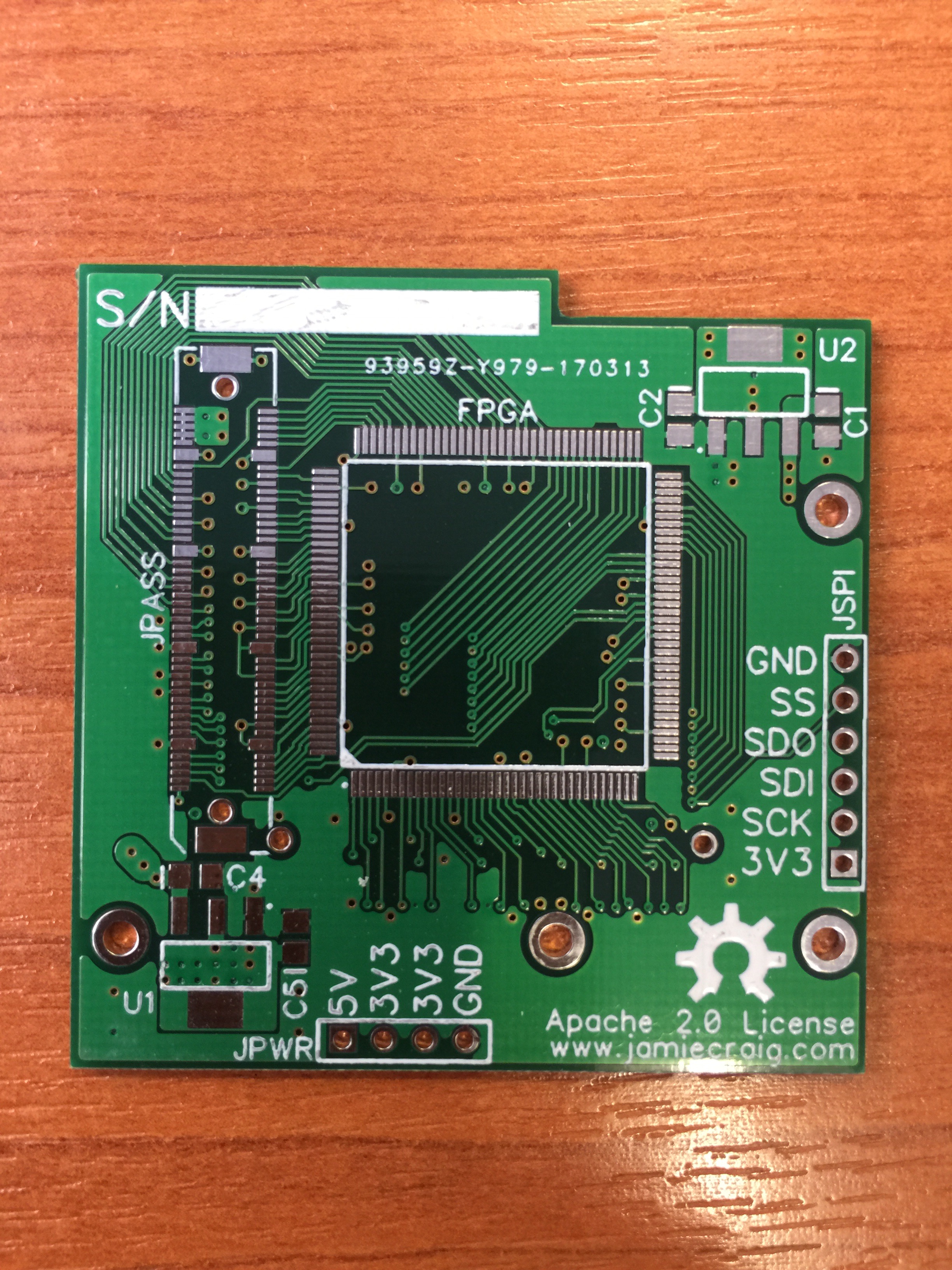
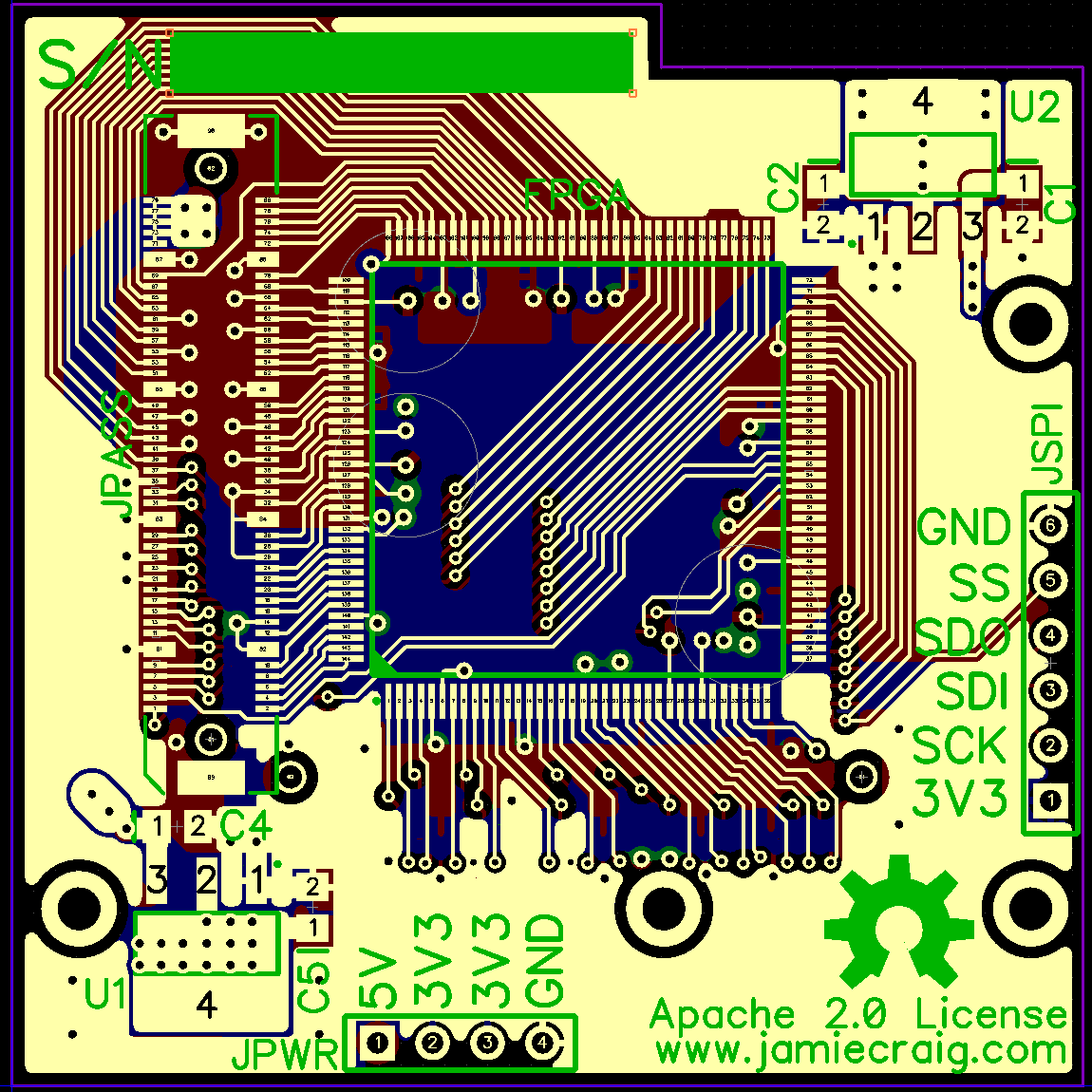
I’ve now got the iCE40 add-on board for the novena up and running. There are a couple of defects on the board design that need corrected before you can get one of these boards to run. These are:

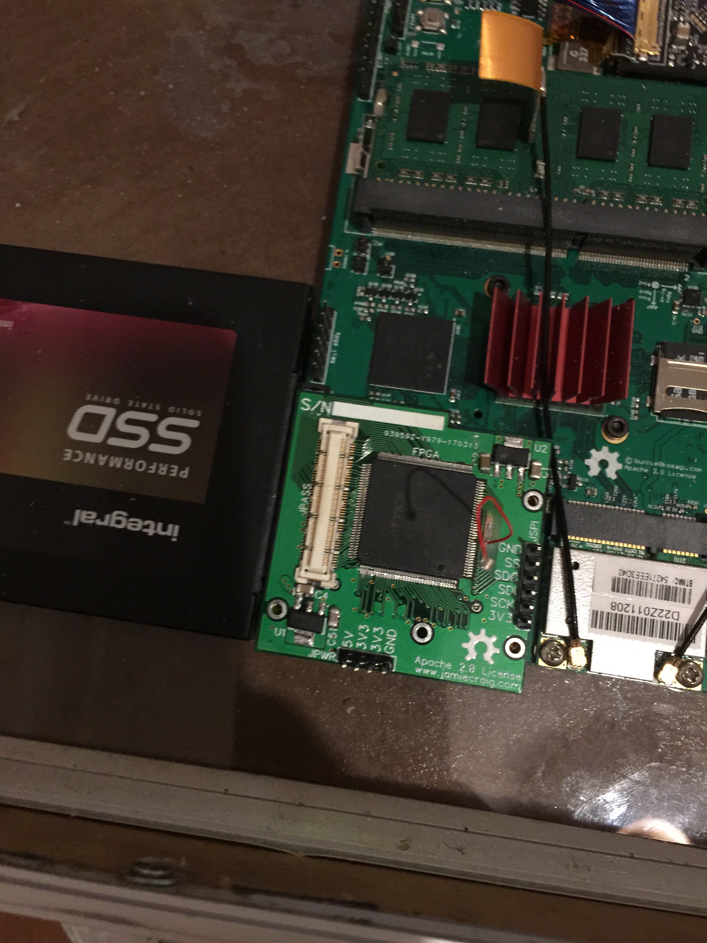
Missing power to the VCC_SPI pin (pin 72, top pin on the right-hand side of the chip, nearest the 1.2V regulator) – this just needs jumpered to any available 3.3V point. Since it’s the very corner pin, there’s no difficulty connecting this by hand.

Bad footprint for the pass-through connector – the FX10A_80P_8 connector footprint I’ve used is too narrow,  and it makes it very difficult to solder by hand. Reflow should be OK as long as the solder resist layer isn’t excessively thick on your boards – the pads are in the right place, just too short.

I’ll do a revision of the board layout when I get some time, but for now, this is pretty functional.

I’ve written a basic loader for the iCE40 , which uses a slightly modified GPBB Xilinx bitstream for now. I hope to write a proper bus bridge for the Xilinx to interface between the two ICs, but for now it’s enough to get blinkenlights working. The sources (and a copy of the compiled Xilinx bitstream) are available here.

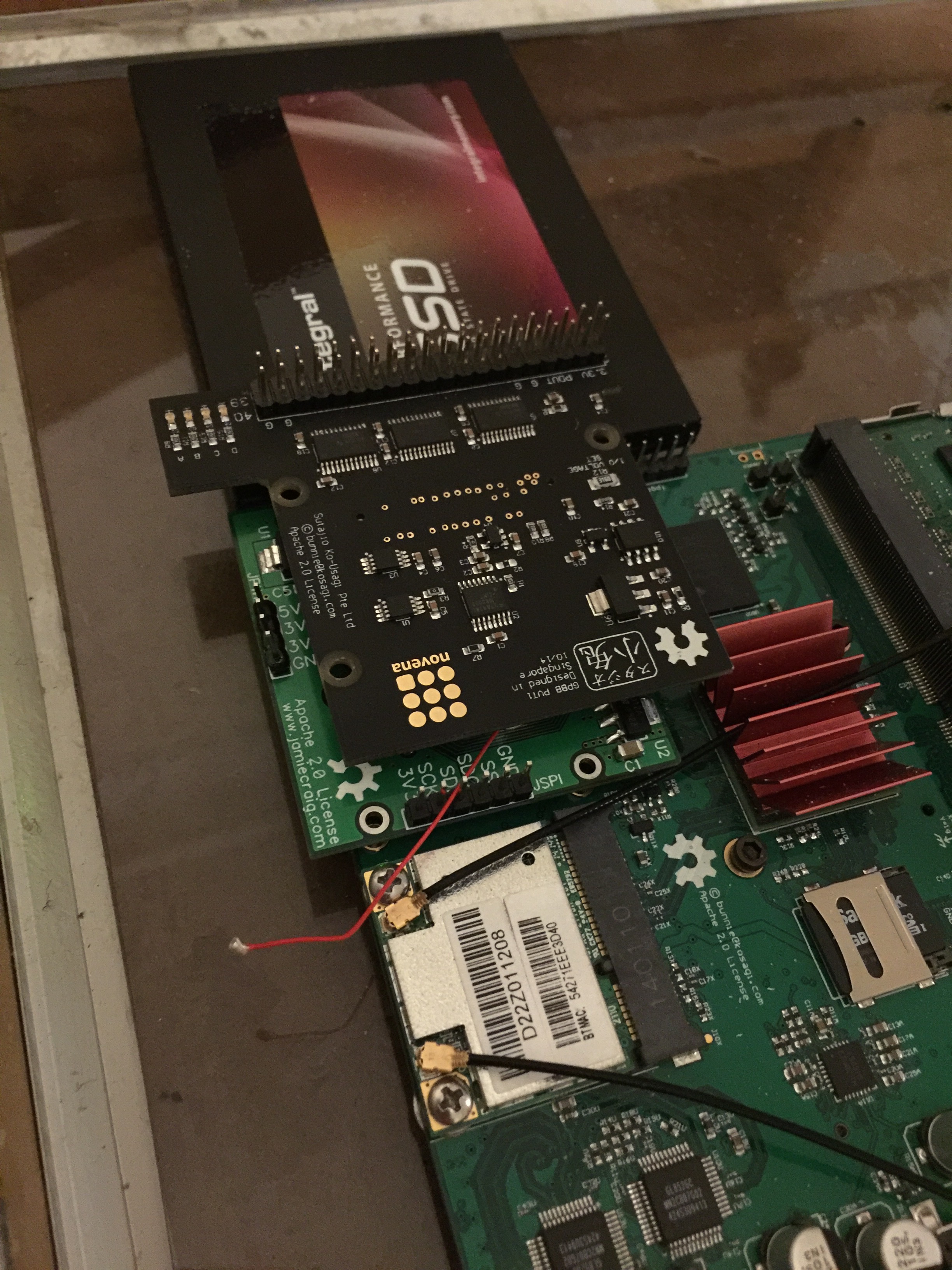
I’ve also included a basic blinkenlights demo for the GPBB when piggy-backed on the iCE40.

Also about this board:

Novena iCE40 Add-On Part 2

I’ve received the boards for the iCE40 add-on back from DirtyPCBs, and they look good. As far as I can tell, everything seems to be functional, although I’ve got some coding to do before I can tell for certain – in particular, I need to put together a bootloader of some sort to feed the SPI port on the iCE40 with the bitstream.

In the meantime, I’ve put together one of these boards and got it powered up in a spare novena to test, and I’ve quickly thrown together enough Verilog code for the Xilinx to be able to bit-bang SPI to talk to the iCE40.

For anyone following along, the only mistake I’ve noticed on these boards has been the wrong footprint for the upper pass-through connector; the one I’ve used is close enough to fit, but there’s some definite overhang on the pins over the pads, and it’d be wise to redo that part if you’re considering making one of these boards.  I’d also recommend using the taller version of the lower connector, as I found the board sits slightly high at one side as a result of resting on the SATA connector. It’s flat enough to still make good contact, however, so if you only have the shorter connectors, you should be OK.

Here’s the board sitting in place in the novena (with a patch wire onto the reset pin during bringup):

and with the GPBB fitted on top:-

Also about this board:

Novena iCE40 add-on

I’ve been working on an add-on board for the Novena open-source laptop, which provides an iCE40HX4K FPGA on a mezzanine board designed to fit in between the Novena and any add-on boards.

The reason this is useful is that Clifford Wolf’s icestorm project provides a fully open-source FPGA toolchain for the iCE40 that can run locally on the Novena, thereby removing the need for an x86 desktop machine when playing with FPGA projects. The Xilinx FPGA will act as a bus bridge between the iCE40 and the Novena, and (hopefully) provide access to RAM too, using a fixed, shared, FPGA design.

picture of the PCB layout for the novena mezzanine board

The board is intended to sit in the same location as the normal GPBB board would in a Novena laptop, and to provide a rotated FPGA header for the GPBB or other add-on boards to connect to, positioned such that it will sit above the SSD. This isn’t ideal, but the Novena layout is very tight for space around the FPGA connector, so it’s the best way I could fit in space for a whole second board.

At this point, I’ve drawn up a PCB design for the board, and I’ve ordered the first batch from dirtypcbs.com to try out. If anyone’s curious to look at the schematics or board, they’re available here in DipTrace format. Everything’s under the Apache 2.0 license, to match the Novena itself.

Also about this board: