Early floppy disks

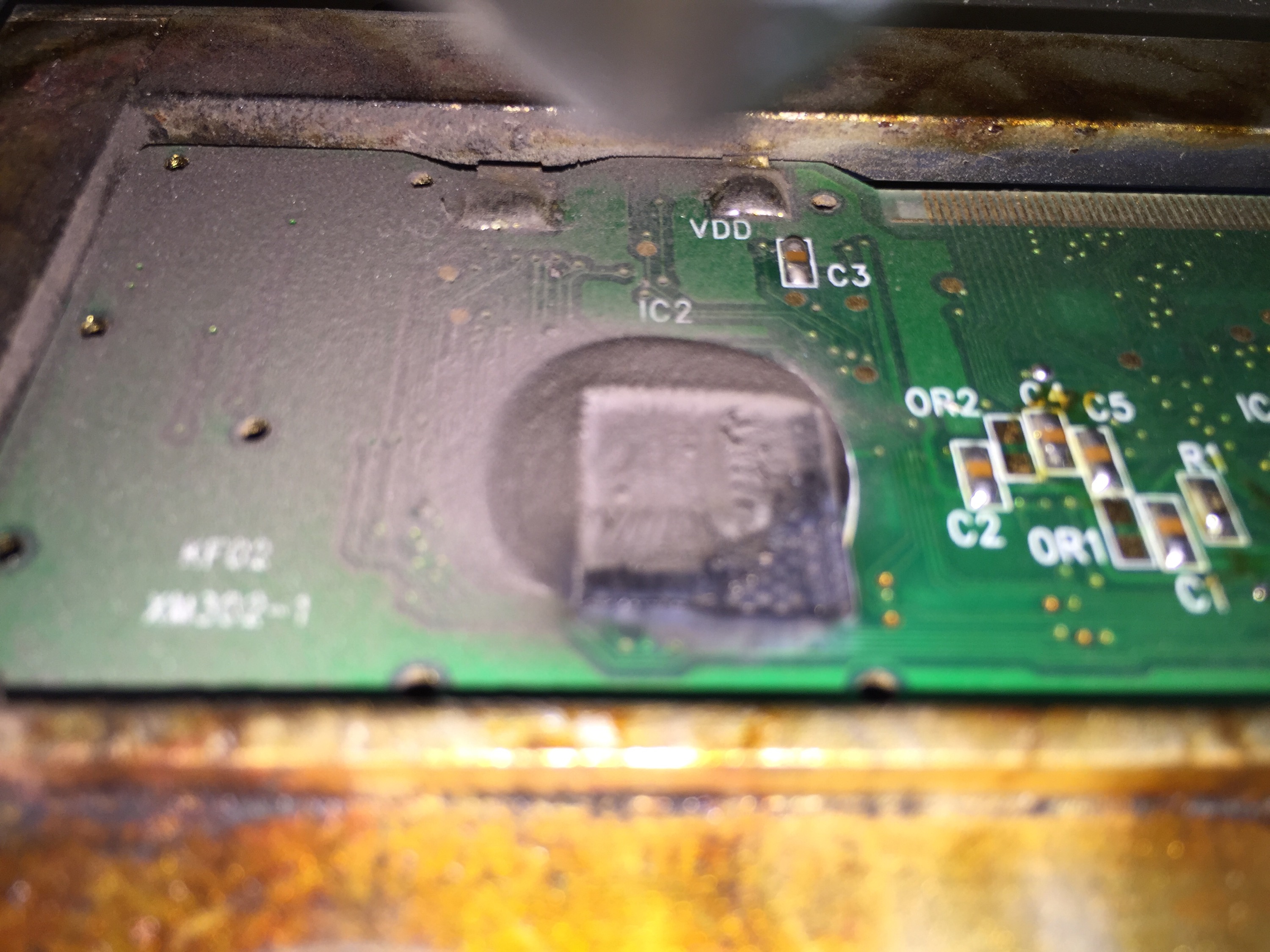
I was talking on IRC to some people today about an old Apricot computer I had, which had some curious features. Among other things, it was PC compatible in all ways except the BIOS, which meant that it needed a special custom version of MSDOS to boot. I remembered, while thinking about this, that I had some unusual very early floppy disks that had come with it. These don’t quite look like your normal 3.5″ floppies, although they’re compatible with normal drives.
IMG_1383.JPG
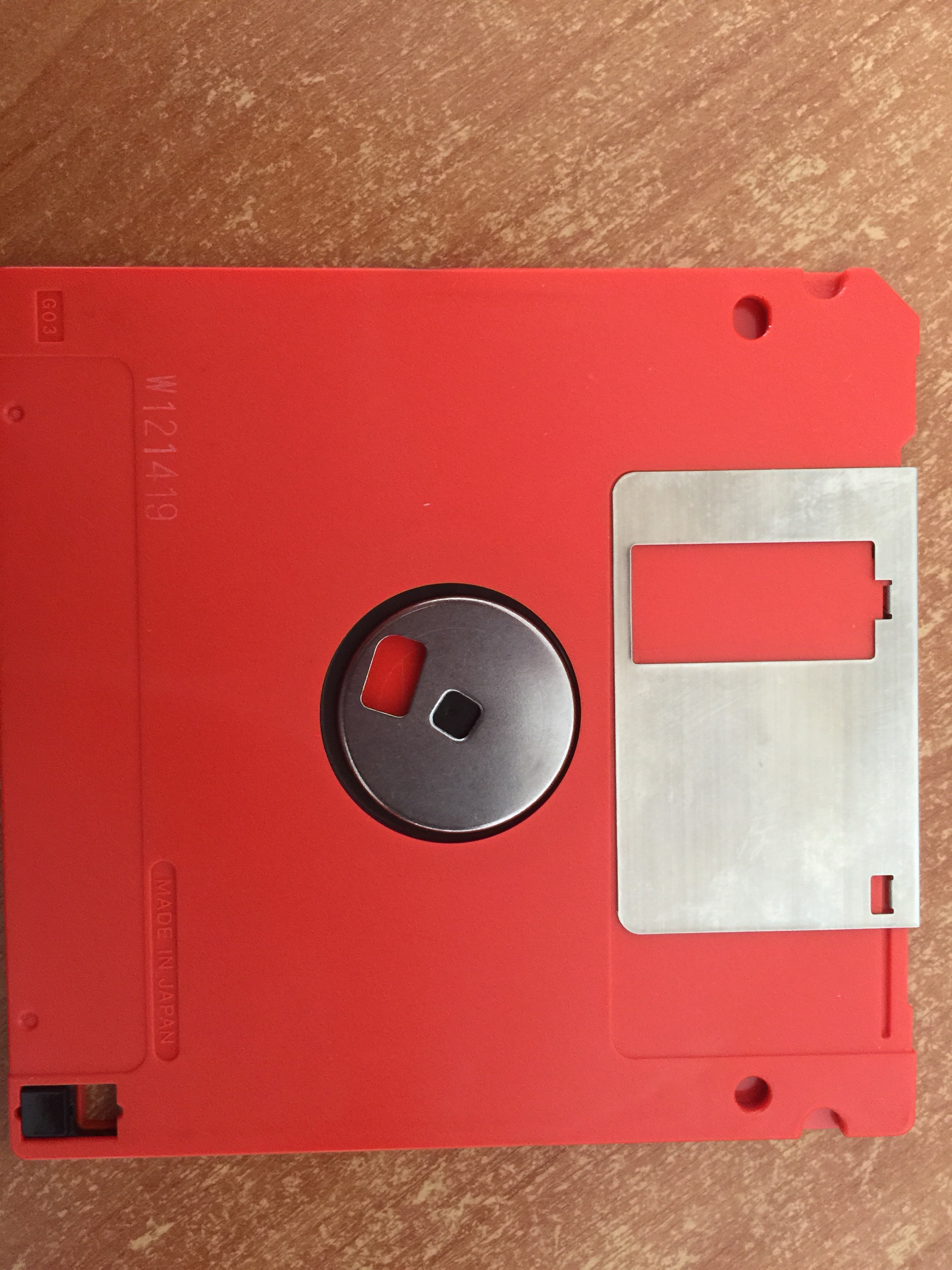
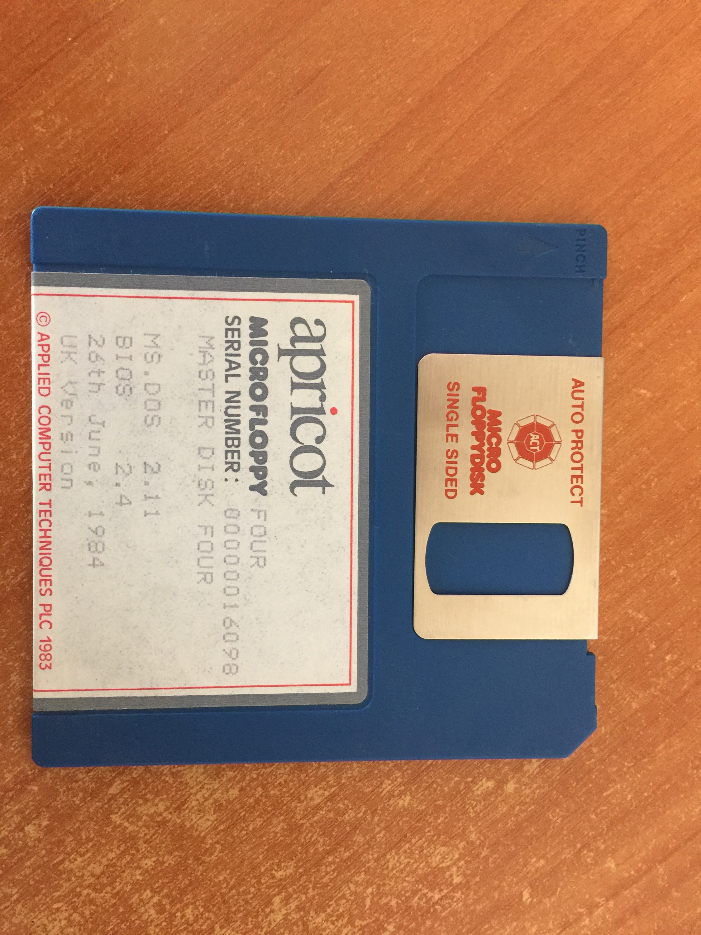
Unlike normal floppy disks, these ones have a latching shutter that can be held open. As far as I can tell, this was so that drives could be made without the extra arm/lever that flicks open the shutter, and therefore would reduce costs a little bit. For some reason I’ve never seen this style of disk anywhere else, so I thought I should photograph one of the ones I’ve got for posterity’s sake.

IMG_1384.JPG

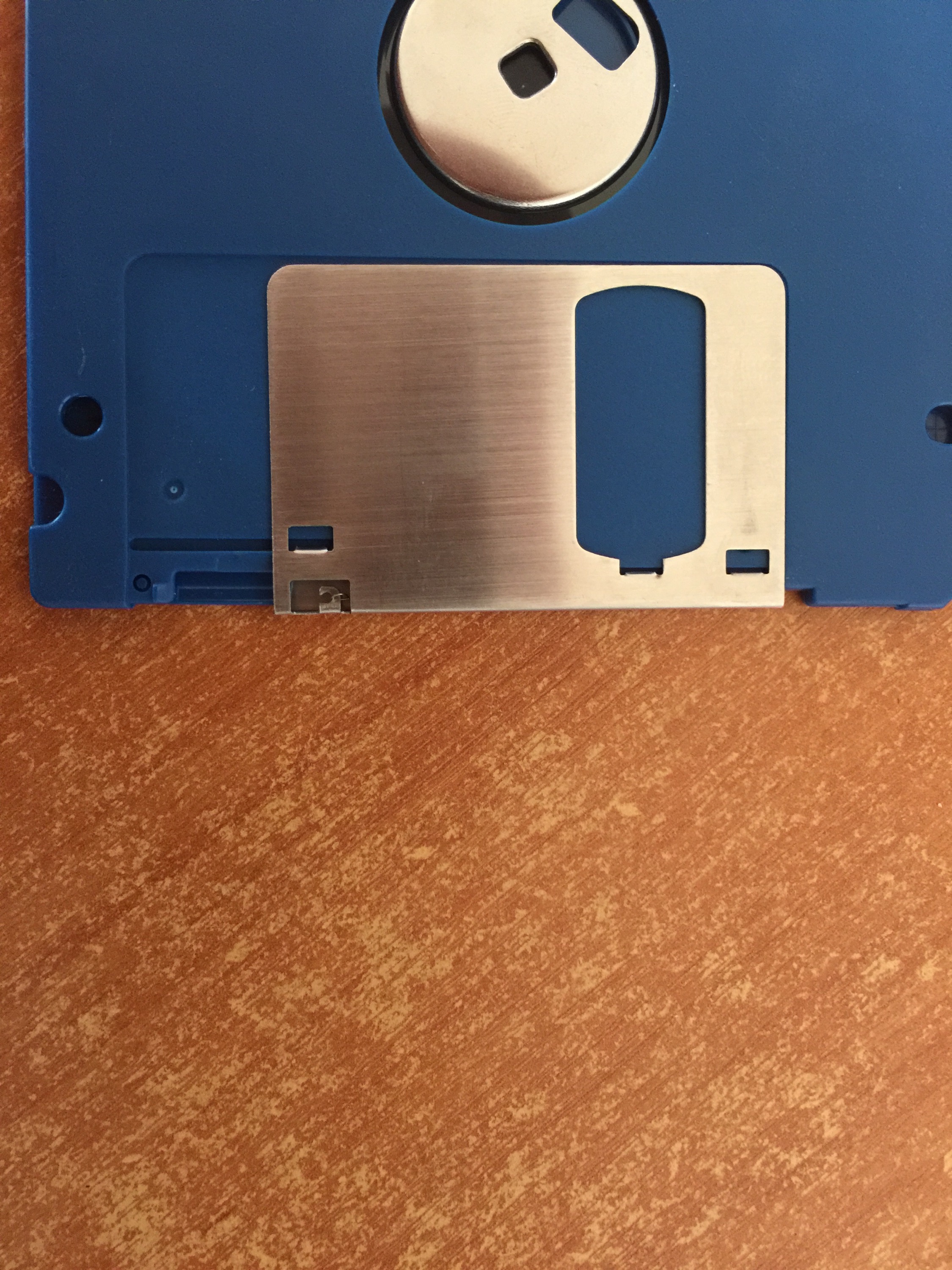
The latch itself is simply made from the plastic of the disk and an extra crease in the metal shutter blades. To latch the shutter open, you just push it open past the normal stop point where a normal floppy drive would push it to; beyond that point, it locks into place. To release it, you just squeeze the corner of the disk, which is slightly split, and the shutter pops closed again.

IMG_1385.JPG

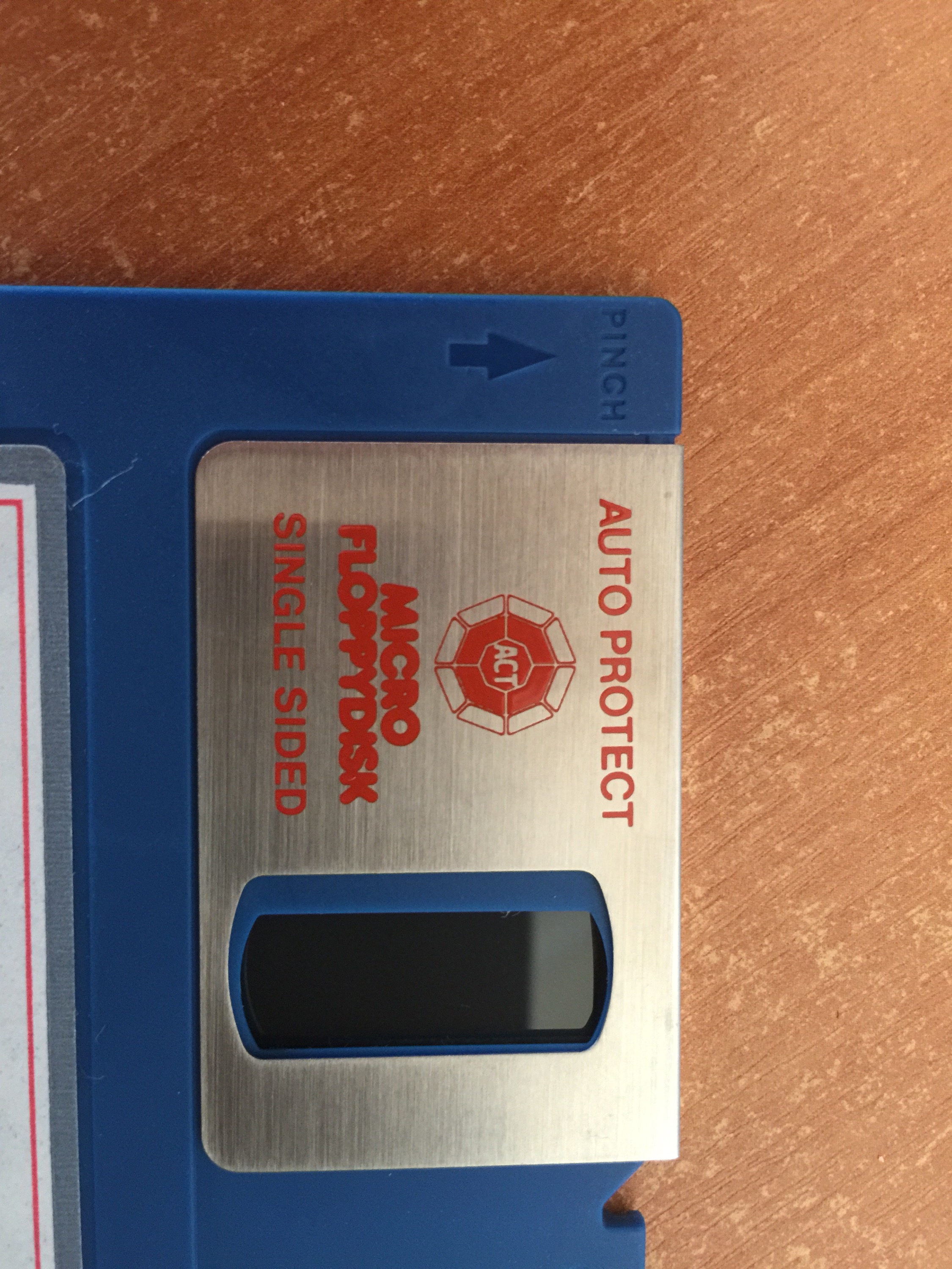
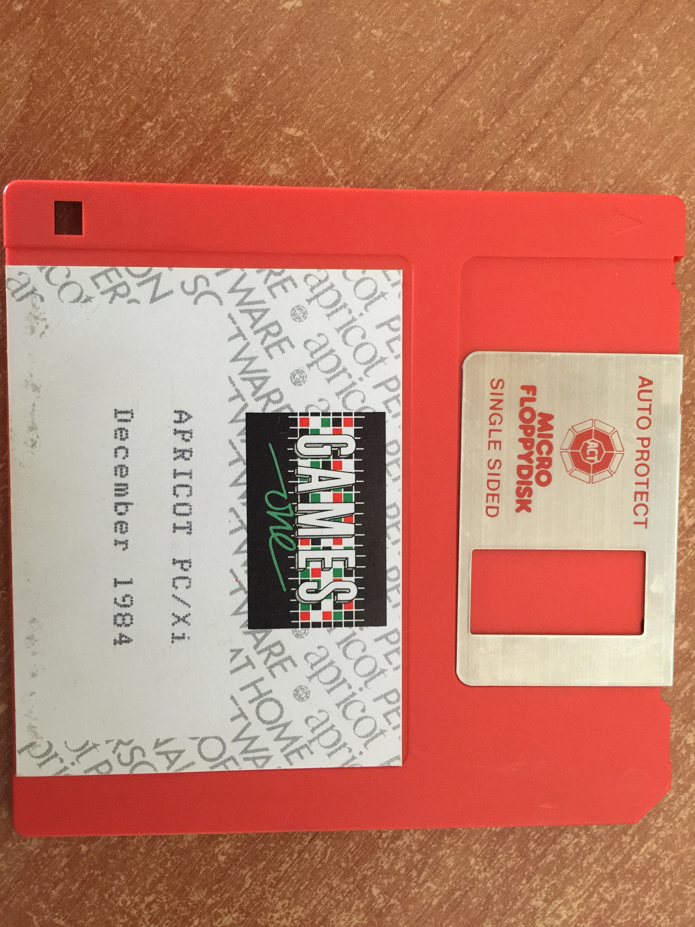
This also makes it a little easier to clean the disk surface if you manage to get some greasy finger-prints onto it somehow (although it obviously increases the possibility of that happening in the first place). I can only suppose that these were really early disks and predated the lever being standard in floppy drives, but I was sure that Sony invented the 3.5″ microfloppy, and that the first ones had that lever. Perhaps some clones omitted that detail for some reason? In any case, it’s an interesting and rare feature.

The same company supplied, at the same time, some disks without this feature too, and my Apricot machine didn’t actually need the latch, just to further confuse matters.

De-encapsulating ICs with a laser cutter

OLYMPUS DIGITAL CAMERA
Closeup of dictionary ROM

I recently found, in an old box of random electronics, a pocket dictionary of the 12-in-one spellchecker variety. The board had two large chip-on-board ICs on it, both covered with the usual black epoxy of doom. The actual traces routing between the two were relatively sparse, and I was somewhat curious what the architecture of the device actually was, so I decided I’d like to de-encapsulate the chips to see what was making it tick.

I’ve heard many times in the past that the best way to do this is by careful application of fuming nitric acid. Unfortunately, that’s somewhat controlled in the UK as it’s considered a precursor for making explosives; as a result, I didn’t have any to hand. However, I thought it might be interesting to try a different approach – a laser cutter.

40W CO2 laser cutterI have a generic 40W chinese laser cutter, of the kind you can pick up cheaply on eBay. This particular laser has been upgraded very slightly with some better stepper control electronics and an air assist nozzle for the head; however, it’s still using all the original optics and laser. The air assist is the only relevant improvement for this job.


I set the PCB with the COB blob up under the laser, and fed in a simple half-inch square bitmap to the laser control software to be engraved. This made the laser perform a raster pattern across the surface of the COB device, neatly etching away the epoxy. If you’re trying this yourself, I used three passes, with the laser at full power and set to 300mm/sec and air assist on.

IMG_1369.JPGA single pass yielded a noticable depth of cut into the epoxy blob, with a fairly good surface; it was a little dusty (the various unpleasant byproducts of burning epoxy tend to recondense on nearby surfaces), but the laser was clearly cutting the epoxy fine. The question was whether it would trash the silicon underneath.IMG_1367.JPG

After the third pass, the die surface started to become visible, and so I stopped and cleaned off the surface with a brush. Unfortunately, I was a little heavy-handed with the brush, and some of the gold bond wires were broken as I did – they were actually intact before. However, I managed to get a pretty good view of the chip surface, and a look at the layout. Apologies for the poor photograph quality – I was using a biological microscope not intended for top illumination, and it has bad flare problems with the reflections from the IC surface.

OLYMPUS DIGITAL CAMERA
View of the whole chip. The pinholes in the corner are from me lining the laser up with where I wanted it to start.
OLYMPUS DIGITAL CAMERA
Sanyo logo on the corner, along with some of the pin buffer structures.

From this, I think it’s pretty clear that this chip is just a ROM of some sort, and any clever behaviour is implemented on the other chip on the board, Unfortunately I managed to shatter that chip while trying a different process for removing it from the epoxy blob of doom, so I have no photographs of that to show.

I hope this helps if anyone else needs urgently to deencapsulate a chip and work out what’s inside it; it’s faster (less than 5 minutes on the laser) and simpler than the nitric acid approach, and while it doesn’t yield a perfect result, it’s good enough for basic identification. Most importantly, the laser doesn’t seem to cut any of the metal on the chip, nor the bond wires, nor the silicon itself, despite chewing rapidly through the black epoxy.