A few years ago, I bought an HP1661CS logic analyzer. This is part of HP’s 1660C series, with an added 2 channel oscilloscope integrated. Unfortunately I wasn’t lucky enough to get one with a network interface included. However, my friend Stephen (of TerribleFire fame) had a similar device but with the network interface included. Having inspected the two ‘scopes, I’ve worked out how to upgrade any HP1660 series scope with what HP call “Option 015” – the Ethernet interface and support for using it over X11, NFS, and FTP.
The differences between the models with and without the ethernet interface are very limited; most of the hardware for ethernet is present in all models. The differences are:
Ethernet-capable models have 8MB of RAM instead of 4MB – this is a simple 72-pin SIMM installed on the CPU card.
The PCB with the keyboard, mouse, and Centronics printer connector is replaced with one that adds an RJ45 socket with appropriate magnetics, and a 10base2 transceiver and BNC socket.
The firmware is replaced with one that includes support for X11.
Of these, it’s clear that the PCB with the extra ethernet hardware is the most challenging; the upgraded firmware is available directly from Keysight and 72-pin SIMMs are widely available. Most people don’t need the 10base2 interface, and the RJ45 10baseT is sufficient. Modern magjacks contain suitable magnetics, and so only that and some appropriate wiring is required.
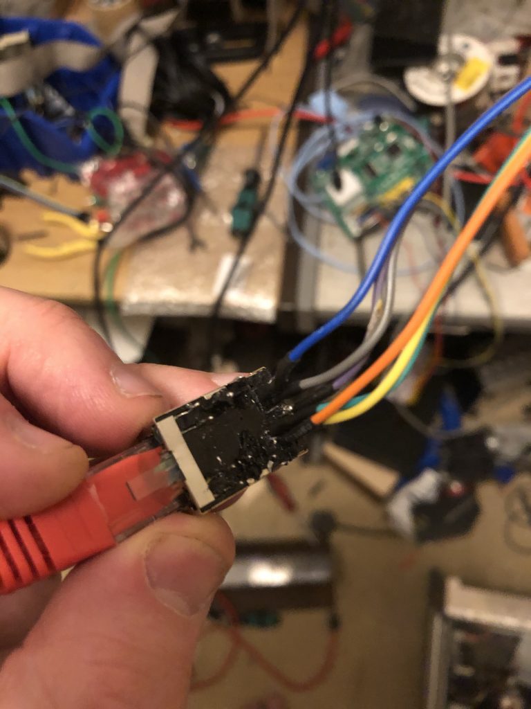
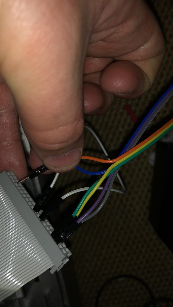
The keyboard/mouse/printer/network PCB connects to the CPU board via a 40-pin IDC connector (i.e. the same ones you’d use for a PATA/IDE HDD). The following connections are required to make the HP1660C detect the network interface and make the magjack work.
Pin 22 to 26 (ground to network interface detection)
Pins 35 and 36 to TX on the magjack (pins 1+3 on the one I used)
Pins 33 and 34 to RX on the magjack (pins 4+6 on the one I used)
Ideally, wire up the grounds on the magjack to pin 22 or 24 (ground)
I actually used a magjack salvaged from an old dead Raspberry Pi. The resulting wiring for testing looked like this:
(Better photos to follow!)
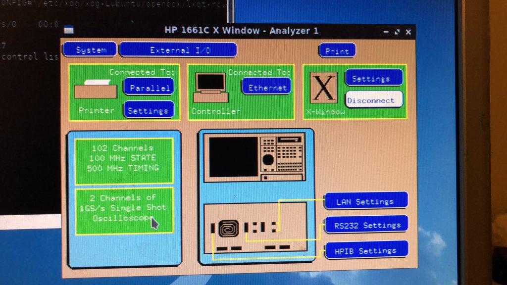
Once the hardware is complete and connected up, and you’ve swapped in an 8MB SIMM, you’ll need to go into the “System” menu, and choose “Update Flash”. With the new hardware connected, the system will ask for SYSTEM.LAN instead of SYSTEM to be provided from the update floppies; run the update and you’re done!
To make best use of the ‘scope once set up, you’ll need a machine running X, and configured to listen for and allow connections from the HP1660’s IP address. In addition it needs some specific fonts installed; these are provided on the firmware disk images from Keysight. If you’re doing this on Xubuntu, you’ll need to create /etc/lightdm/lightdm.conf.d/listen.conf and add the following:
[SeatDefaults]
xserver-allow-tcp=true
You’ll then need to allow the specific IP for your analyser using xhost +192.168.1.123 or similar. Finally, you can start the connection from the LA.
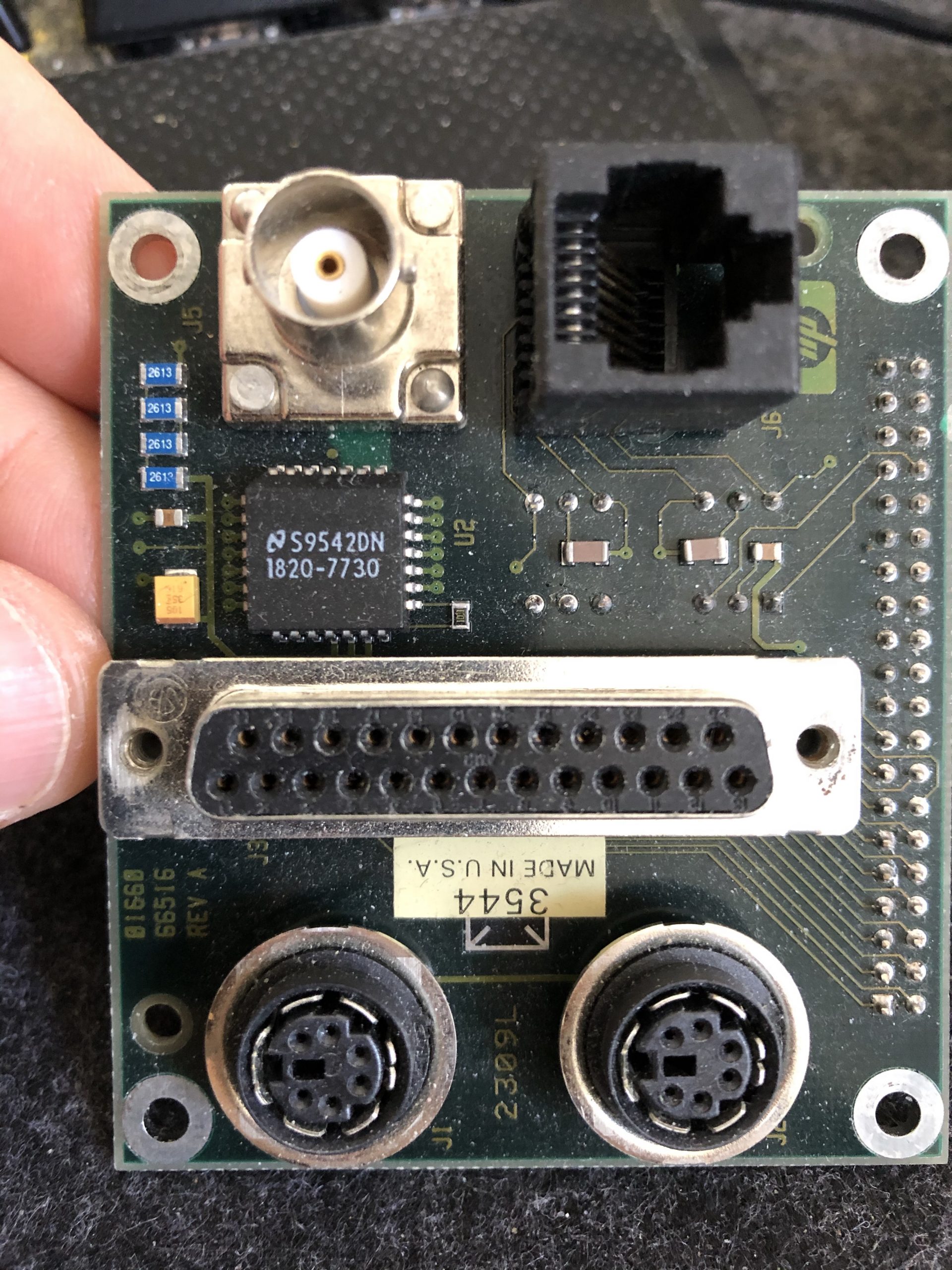
Edit: I’ve had a couple of requests for some photos of HP’s own board for this. Here you go!
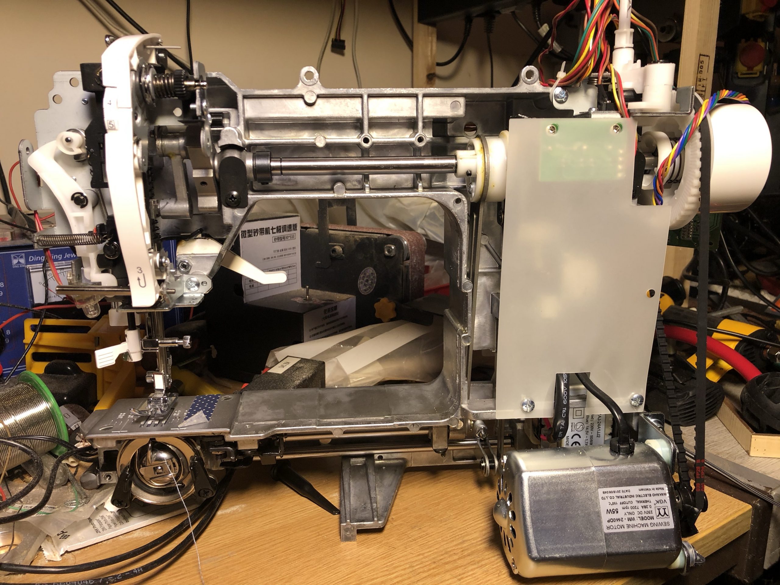
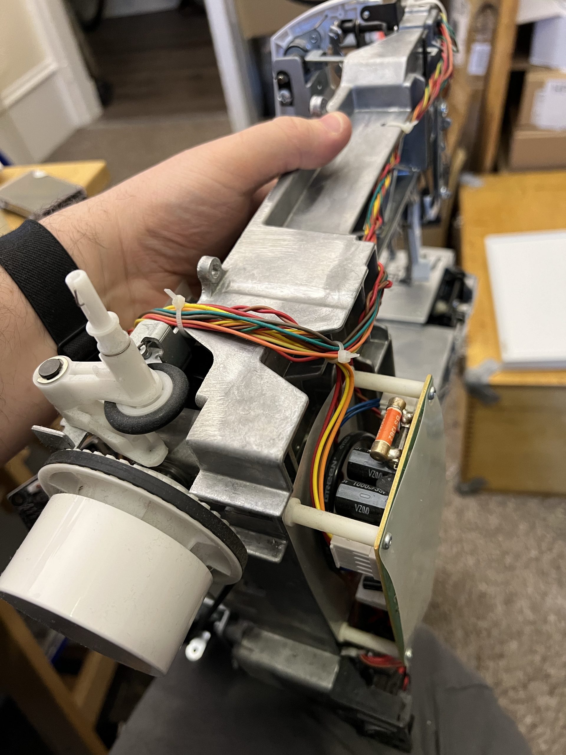
My girlfriend bought herself a Singer Brilliance 6180 sewing machine from Lidl last Christmas. This turned out to have been a big mistake; it’s one of the least reliable and most annoying sewing machines to use in the world. Having replaced it with a vintage machine from the 1980s, she gave up on the 6180, and passed it to me to play with. Of course, I did the obvious thing and dismantled it immediately to see if any of the problems were electronics-related rather than purely mechanical issues. As it turns out, there are some problems in both categories, but there’s a lot of potential for hacking this machine.
Mechanics
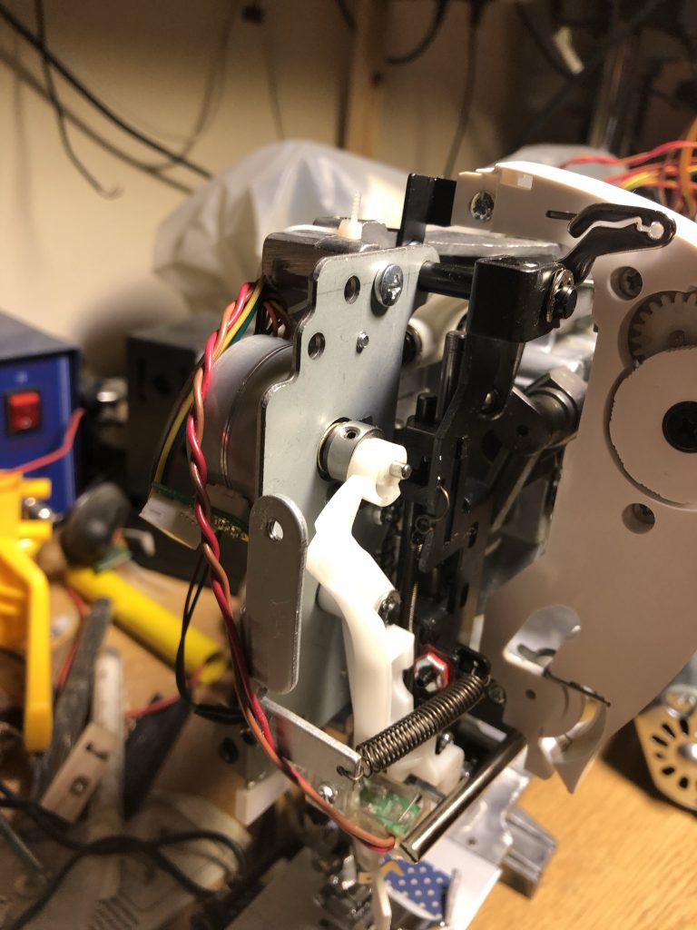
The machine itself is based around a die-cast chassis, with a very basic and conventional sewing machine mechanism with a front-loading bobbin. The mechanical parts of this machine could be considered to be a slightly tweaked straight-stitch only sewing machine, and indeed if you could power the motor without the normal control board, it would function perfectly well like this with no electronics involved. The electronic parts exist primarily to control two small stepper motors; one which moves the needle left-to-right (X-axis, essentially), and one which changes the stitch direction and length by adjusting the position of a lever that controls the feed dogs. Of course, to time movement of these parts correctly, there are also some feedback sensors, and a limited amount of control of the main motor.
The biggest problem – the X axis
The X-axis motor turns a simple plastic cam to move the needle left-to-right, with only spring pressure to return it.
This machine has a few problems, but the most severe by far is the tendency for the needle to fall out of alignment left-to-right and break. This can happen whenever the fabric presents any resistance to the movement of the needle, or whenever the machine is running quickly.
The underlying problem here is that the left-to-right movement of the needle is controlled by lever pushing on a cam attached to a stepper motor with a fairly weak spring to keep it in contact. Any sideways pressure away from the cam – or even the momentum of the assembly – can cause the needle to be out of position, and this quickly leads to needle breakage or jams. In addition, there’s no feedback or zeroing mechanism on this axis – it relies simply on hitting the endstop during startup or the first time the needle is in the “up” position (more on that later). It appears that there’s some provision in the electronics for a limit switch, but it’s not used on this model.
Y-axis
The Y-axis, by comparison, is better engineered. The Y-axis motor turns a gear, which in turn moves a toothed cam, which is attached to a lever that shifts the relative timing of the feed dogs. A proper limit switch is present, and during startup or the first time the main shaft passes a safe point (6 index slots past the start of the unsafe period), this motor will zero itself and then move to the appropriate position for sewing. A mechanical stop identical to that on the X-axis also exists; this suggests that the two axes may originally have have the same setup, but that the X-axis was simplified as a cost reduction.
Speed control
The motor in this machine is not controlled directly by the user. Instead, the electronics generate a PWM signal to select the appropriate motor speed. A relay is also present as a motor enable/disable. It’s not clear why this is required; perhaps it’s simply a safety feature to ensure that the motor is disconnected from power whenever it’s not intentionally being controlled by the processor. The pedal is a simple 20K variable resistor, wired as an input to the main processor. A second speed control input also exists, which is not used on this model, but which sets a speed limit on other machines based on the same chassis and electronics (e.g. Stylist 7258).
The main shaft has two slotted opto sensors connected to it. One is connected to a simple slotted wheel, to provide position feedback on the shaft. The other one detects a disk which provides a needle up/down signal; the disk blocks the sensor whenever the needle is down far enough for it to be unsafe to move it left to right.
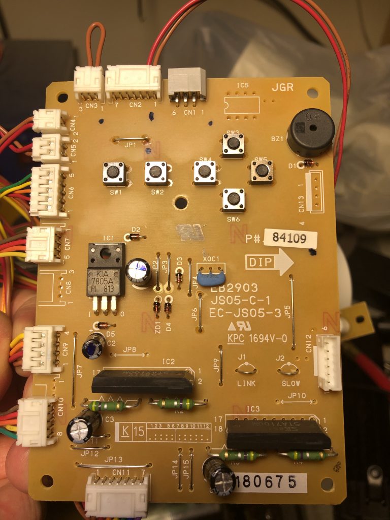
Electronics
There are two large PCBs in the Brilliance; one power supply input board, which also contains the motor speed controller and switching relay, and one with the main processor, keypad, and stepper drive electronics. The power supply board provides only a 20V supply to the main control board, and accepts two control signals; one for the motor relay, and one for the PWM control. These two signals are pulled up to 12V by the power supply board, and are active-low, so the control board has a simple transistor connected to each to pull them low in response to a signal from the microcontroller.
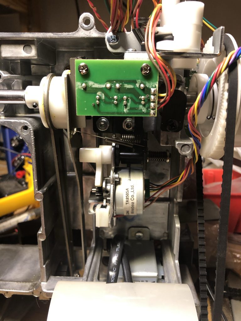
The stepper controllers on this machine are Sanken STA7100M parts. Unfortunately I’ve been completely unable to find a datasheet for these parts. In this particular device, they’re set up as unipolar stepper drivers – i.e. 5 wire, with a centre tap on each coil commoned together.
The microprocessor is, unfortunately, a custom marked device and I haven’t yet worked out which device it’s based on. A 10MHz ceramic oscillator provides the main clock for the chip, and it’s powered from a conventional 7805 linear voltage regulator.
Hacking
One very simple modification that can be made is to connect JP1, which was cut on my machine, to convert it from an 80 stitch machine to a 100 stitch machine. No further change – except to the stitch chart so you can tell what the stitches now are – is required!
My intention is to replace the control board in this machine with a 3D printer control board, which already provides for appropriate stepper drivers and control signal buffers. With the main motor control wired to the -ve side of a heater control pin, there’s no reason why a 3D printer board like a RAMPS (or, as I’m using, Makerbase SGEN-L) would need any modification to control this sewing machine. The biggest complication is the wiring of the steppers, where a track must be cut on the stepper connector PCBs to decouple the centre taps.
To help anyone else interested in doing such a project, I’ve mapped out the connectors on this machine, and a full table of connections is below. I’ve used the pin numbering marked on the board; be careful when using this, because the numbering runs in opposite directions on some connectors relative to others (because the inverted orientation is used on some to avoid misconnection during factory assembly).
Connectors
All of the connectors in use on the control board are around the periphery. The connector orientation and pitch is deliberately varied between so that no connector exactly matches any other – this ensures that during assembly (or reassembly!) you can’t really get it wrong.
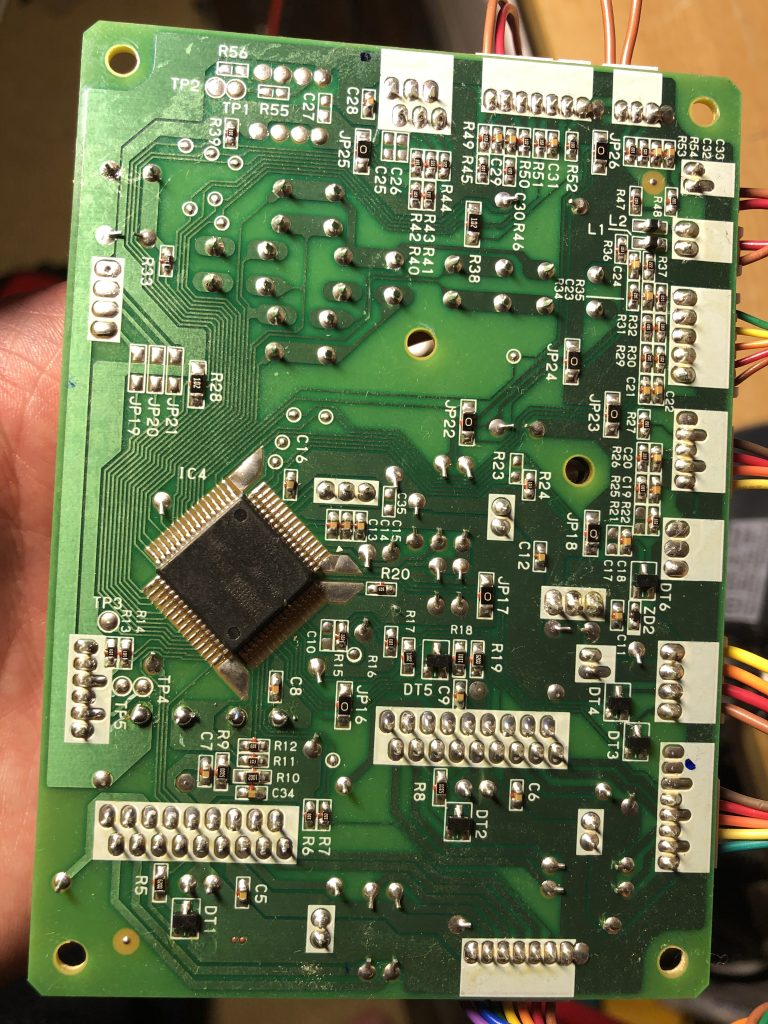
On the top of the board, there’s two stepper controllers, a 7805 regulator, a crystal oscillator, the buttons, a buzzer, and a handful of discrete components. On the underside there’s the microcontroller and a fair number of discrete transistors and passive components.
CN1 – LCD connector
The LCD on this machine appears to be an SPI device, or sufficiently similar to present signals that look like it. This is a zig-zag pinout on the board.
1
5V
2
Ground
3
Data (MOSI?)
4
Clock (seems to run at 200kHz normally)
5
5V
6
CS
CN1 – LCD connector pinout.
CN2 – Reverse Switch
This is a 7 pin connector, but only 2 pins are used in the Brilliance 6180. The first two pins are connected to the reverse switch. The others appear to be wired appropriately for other buttons; perhaps another model has more inputs?
1
Reverse switch (has 1K pullup on board)
2
Ground
3
4
5
Ground
6
7
CN2 – Reverse switch pinout.
CN3 – Speed control header
This is a 3-pin connector which is clearly intended to be connected to a slide potentiometer in other models. A simple wire jumper between the first two pins is present on the 6180; if you look at the Stylist 7258, a very similar model, you can see where there is a speed limiting control present instead.
1
5V
2
input signal
3
0V
CN3 – Speed control header pinout. Pins 1 and 2 are normally jumpered together on the 6180.
CN4 – Winder Switch
There is a bobbin winder on this machine, and there is a switch to detect when it is engaged – presumably to stop the machine automatically when the bobbin is full. This is a simple switch input with a 10K pullup to 5V present on the board.
1
Winder Switch (pulled up 10K to 5V)
2
Ground
CN4 – Winder switch pinout.
CN5 – Pedal input
This is a 2 pin connector with 5V and the pedal present. The pedal contains a 20Kohm variable resistor, and is configured so that it presents 20K when the pedal is up, and approximately 200 ohms when fully depressed.
1
Pedal
2
5V
CN5 – Pedal input connector pinout.
CN6 – Buttonhole switch
The Brilliance 6180 features an automatic button-hole device. This consists of a special foot, and a lever that mates with it and which extends down from the machine. This lever has two switches mounted on it. One detects when the lever is extended down to mate with the foot; the other detects whether the lever is in the neutral position or being pushed forwards or backwards. The control board interfaces with these switches in the normal way; all are connected with 10K pullups and short the input to ground.
1
Ground
2
Ground
3
Switch input (closed when lever pushed towards user)
4
Switch input (closed when lever pushed away from user)
5
Lever up/down (open for up, closed for down)
CN6 – Buttonhole mechanism switch input.
CN7 – Shaft sensors
The two slotted opto sensors on the main shaft are connected here. It’s important to note that the opto sensor LEDs are powered directly from the 20V input supply (via 620 ohm resistors on the sensor PCB) and not from the 5V logic supply. Note that it’s a 5 pin layout on the PCB, but only a 4 pin connector was present on the PCB (connected to pins 2-5).
1
Not present on my machine
2
Rotation sensor (10K pullup to 5V)
3
Safe-to-move-needle sensor (10K pullup to 5V, open when unsafe)
4
Ground
5
20V
CN7 – Shaft slotted opto sensor connector pinout. Be careful, 20V is present here!
CN8 – Unknown
There’s a 3 pin header marked CN8 on the board, but on my machine no connector is present. There’s no obvious connection to the third pin here, and so it’s not clear what this could have been for. Perhaps as an LED power supply on a different model?
1
Ground
2
20V
3
N/C?
CN8 – Unknown header pinout. 20V present here.
CN9 – Power supply and speed control
CN9 is the main power input to the board, as well as providing connections to the speed control inputs on the PSU board. On the control board there’s a transistor between each of these inputs and ground. They appear to have a 12V pull-up on the PSU board.
1
Motor relay (short to ground to enable motor)
2
Motor PWM (short to ground to power motor)
3
Ground
4
20V
CN9 – Power supply input and speed control pinout
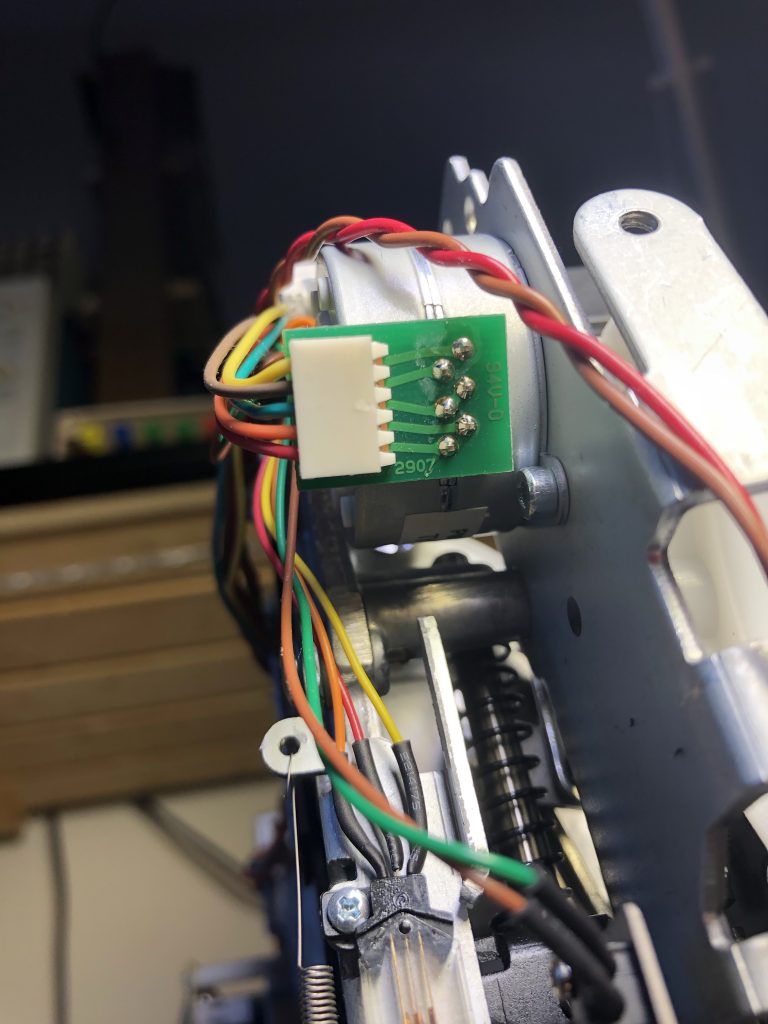
CN10 – X-axis motor
CN10 is an 8-pin header on the board, but only a 5 pin connector is actually present on my machine. The pinout appears to be similar to CN11, the Y-axis motor, but the limit switch is not present and a smaller connector used as a result.
1
Not present
2
Not present
3
Not present
4
Coil
5
Coil
6
Coil
7
Coil
8
Common centre tap
CN10 – X axis motor pinout
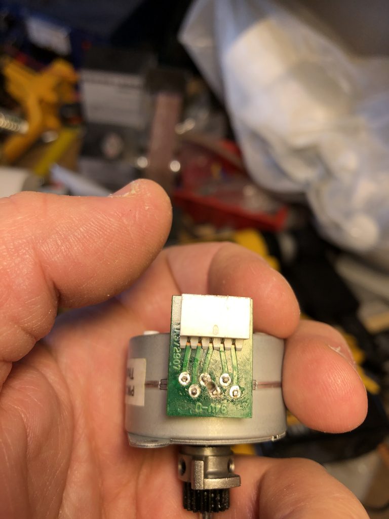
The motors used are actually 6-wire types, but the centre taps are connected together on the small header PCB that interfaces the motor to the cable leading back to the control PCB.
Motor header PCB
The motor used is a Minebea PM35L, which is a 7.5-degree-per-step motor, with a current rating of 500mA. Because it’s wired as unipolar motor, if you want to use it with standard 3D printer stepper controllers, you’ll need to modify the motor connector PCB. I found the easiest way to do this was by drilling out the track (which exists on both sides of the board!) linking the two centre-taps.
Motor connector PCB with the centre tap connecting track (present on both top and bottom of the PCB) cut by drilling it out.
CN11 – Y-axis (feed dog control) motor
CN11 is connected to the feed dog control motor, and to the limit switch that controls the zeroing of this axis. This is a 7 pin connector.
1
Ground
2
Limit switch (10K pullup to 5V on control board)
3
Coil
4
Coil
5
Coil
6
Coil
7
Common
CN11 – Y-axis/feed dog header
The Y-axis motor is identical to the X axis motor, and with the same modification required to use a normal bipolar driver.
CN12 – Unknown
CN12 is a vertical header, unlike the 90 degree headers used for everything else on the board. Its placement somewhat in from the edge suggests that this may be a programming connector, used only during production. It’s not clear what’s actually intended to be wired to this.
CN13 looks to be some sort of debug connector. It’s not populated on my board, and all of the pins connect to a set of also unpopulated resistor pads that would connect them to the microcontroller.
1
N/C
2
Connects to JP21
3
Connects to JP20
4
Connects to JP19
CN13 – Debug Header pinout.
Edit: One visitor asked me about the possibility of replacing the power supply fuse. Here’s a picture showing the location of the power supply board and the main fuse. Unfortunately it’s soldered in – I ended up replacing mine with another (somewhat inappropriate) fuse after popping it a few times by accident.
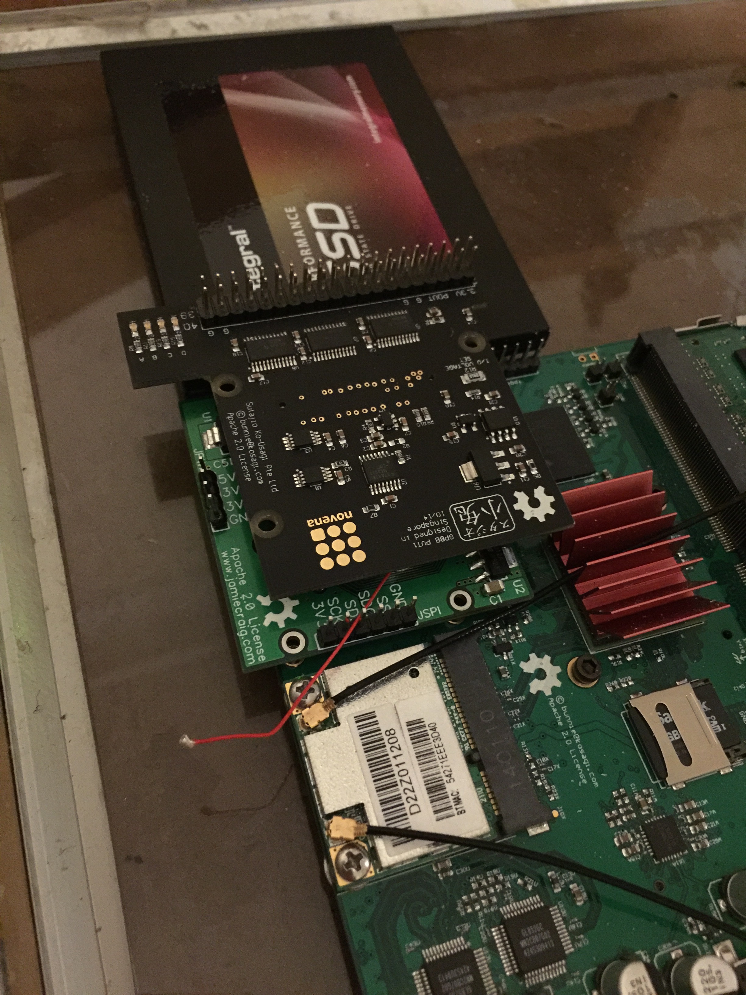
I’ve taken the existing Novena iCE40 add on board and made some minor improvements to the layout. In particular I’ve connect up the few stray signals where I didn’t have space to route previously, and replaced all the 0402 components on the rear surface.
One of the very few complaints I have with the Novena laptop relates to the positioning of the FPGA header on the board. The header is next to an edge of the case, which is important for devices that need external I/O headers, but unfortunately it’s nowhere near the Novena’s Peek array, and therefore hard to combine with internal add-ons. (It’s also a bit close to the CPU heatsink and wireless cards, so you can’t easily use large boards on the FPGA header).
To work around that somewhat, and to try and address some wish-list features I’d have liked on the general-purpose breakout board on the Novena, I’ve been toying with the idea of a bus breakout of sorts, designed to sit in the Peek array, and provide a few buffered I/O slots. Ideally, we want an iCE40 FPGA in there too, to make it easier to build custom FPGA code directly on the Novena – to build for the Xilinx part needs the proprietary Xilinx tools running on a remote machine.
I’d set myself a few basic requirements before starting designing a board for this;
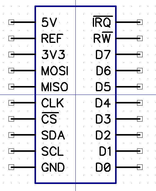
Add-on devices can appear memory-mapped into the Novena’s address space – this is one of the unique abilities of the Novena FPGA slot vs. devices plugged in over USB or I2C.
Add-on devices should be able to be 3V, 5V, or any other reasonable voltage without needing to incorporate level-shifting buffers into the device (so you can, for example, use simple 74-series buffers as GPIO for either voltage, selectably)
At least two, and preferably more, add-on devices should fit into the Peek array, and be able to be mounted securely.
0.1″ pitch headers, only, so that add-ons can be made up on Veroboard or perfboard.
I2C, parallel data, and SPI should all be supported (at any voltage).
When I mentioned some of the details of what I was planning on IRC, Sean Cross (xobs) noted that he’d been considering building something similar with an iCE40 as a catch-all factory test device. I realised that nothing about Pi connectivity fundamentally clashes with the Novena requirements, so I’ve been experimenting with board layouts to try and accommodate both. For the raspberry pi, the main way to talk to the device will be over the SPI port, with both chip selects on the Pi connected up and usable. The same SPI interface allows both reprogramming the FPGA and communicating with it after setup (using two different CS pins). For the Novena, the same approach can be taken, using the SPI port brought out to the front panel board. It’s also possible to use some of the GPBB pins as another SPI port. In both cases the Xilinx FPGA can mediate and present whatever’s attached to the iCE40 as a memory-mapped device. Several extra pins are connected to allow QSPI, UART, and I2C interfaces between the host computer and the iCE40. Of course, since the Pi connector’s pins all go into the iCE40 FPGA, there’s no real requirement that the protocol spoken is SPI at all!
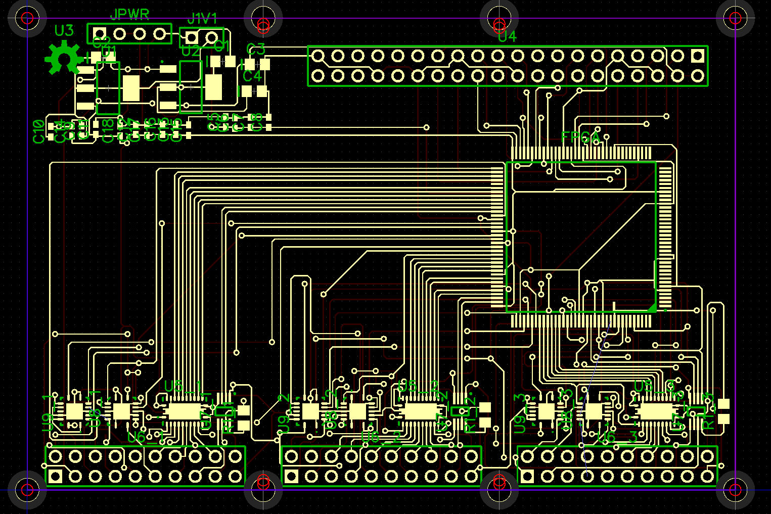
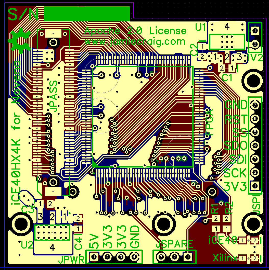
My current work-in-progress is based on a board that fits in a 90mm x 60mm region of the peek array, as shown below, and provides three slots on 30mm spacing. To allow add-on boards as much room adjacent to each other as possible, and a secure mounting directly to the peek array, the boards have notched corners, and a single screw in each corner (which may be shared with the adjacent board) secures them.
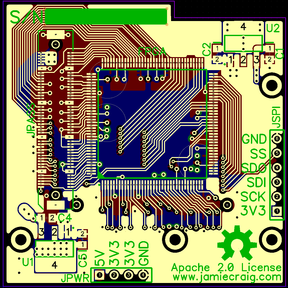
My current proposed pin-out for each slot includes a reference voltage pin sandwiched between a 5V pin and a 3.3V pin; this allows a simple jumper to be used to select a suitable voltage, or an external regulator can be used to feed some other reference into the reference pin. Each slot has I2C, SPI, a simple 8-bit bus, and an interrupt pin to allow it to signal for attention.
The 8 bit data pins are connected to a bidirectional (switched) level shifter, which can therefore be used for QSPI as well as for a normal 8 bit bus. The other pins are wired to single-direction level shifters as appropriate for the signal role.
As a first “will this even fit” test, I’ve dropped all the key components onto a PCB layout and run the DipTrace autorouter against it; this succeeds even on a 2 layer board, so this design looks achievable. I’d love to hear any feedback on the idea; you can reach me as MadHacker on #kosagi at irc.oftc.net, at the obvious email address, or you can leave a comment below.
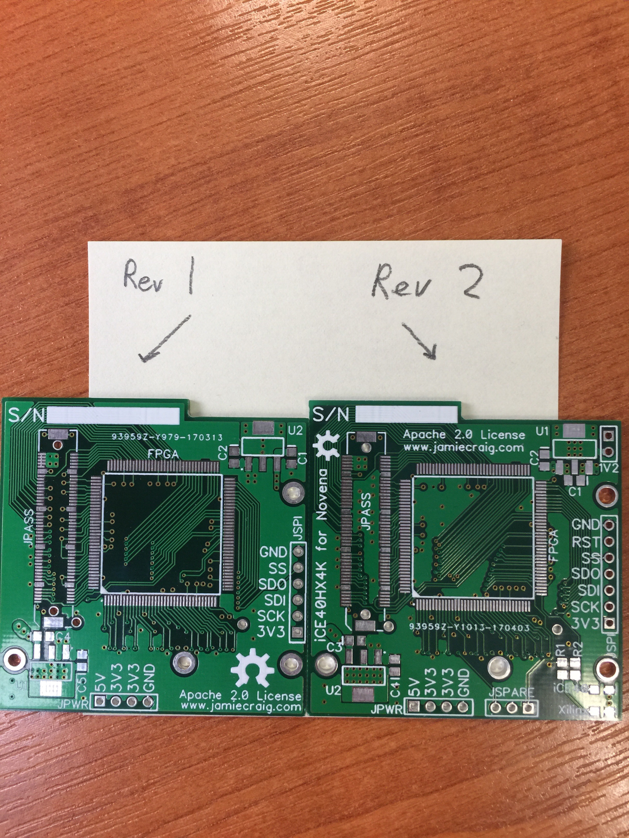
Today, I got the revision 2 boards back from DirtyPCBs, and they work well. The new pads for the FX10 connectors line up much better, and the FPGA started up first time without any trouble. The extra connectors make it a bit easier to debug, or to use the board without a Novena attached. The larger-diameter mounting holes also make it much easier to attach. At this point, I’m happy to declare these boards a success; now I just need to get some Verilog written for the bus-bridge between the Xilinx and iCE40 FPGAs.
To help anyone else writing code to run on these boards, I’ve written a spreadsheet that’ll allow you to map the iCE40 FPGA pins to the Novena standard name for them, and to the GPBB role, on both sides. It will also produce the set_io statements for IceStorm’s .pcf constraints files, which simplifies getting something up and running quickly.
I’m not intending to manufacture any of these for general supply, but if anyone else is interested in these boards, you can get the bare PCBs from DirtyPCBs (file’s already uploaded and ready to go at this link – I’ve set up a zero cut for myself, so you’re only paying DirtyPCBs prices, no extra fees for me). The rest of the parts are listed in the BOM and are all available from both RS and Farnell – I’m sure the usual other suppliers will be able to provide something suitable as well. As the board is under the Apache 2.0 license, there’s no problem if anyone else wants to manufacture for others – feel free.
As I make progress on the bus bridge code, I’ll post it here, but in the meantime, have some blinkenlights. 🙂
I’ve now redrawn this board to correct the problems found with the previous version, and the new board’s schematics and layouts are now available at this link. As well as correcting the problems I had before, I’ve also managed to add in a few extra features. I’ve found two pins from each FPGA that weren’t sensibly routable, and connected one to an LED and one to a 0.1″ header for each FPGA. This helps a bit with debug, as you can more easily see what’s going on. I’ve also added the FPGA reset pin to the SPI header, which means that it’s now possible to bring up the FPGA without a Novena attached. Previously, you couldn’t do this because you couldn’t bring the FPGA out of reset without a bodge wire, but the extra pin makes it straightforward. Finally, I’ve added a 1.2V header, so you can access the FPGA core voltage if you want.
I’ve uploaded the schematics as a PDF as well as the original DipTrace and Gerber files in case anyone wants to take a look without having to download Diptrace.
The new board is, as before, under the Apache 2.0 license. I’ll be getting a few of these made up at Dirty PCBs, and will post again here when I’ve got one assembled and tested.
I’ve now got the iCE40 add-on board for the novena up and running. There are a couple of defects on the board design that need corrected before you can get one of these boards to run. These are:
Missing power to the VCC_SPI pin (pin 72, top pin on the right-hand side of the chip, nearest the 1.2V regulator) – this just needs jumpered to any available 3.3V point. Since it’s the very corner pin, there’s no difficulty connecting this by hand.
Bad footprint for the pass-through connector – the FX10A_80P_8 connector footprint I’ve used is too narrow, and it makes it very difficult to solder by hand. Reflow should be OK as long as the solder resist layer isn’t excessively thick on your boards – the pads are in the right place, just too short.
I’ll do a revision of the board layout when I get some time, but for now, this is pretty functional.
I’ve written a basic loader for the iCE40 , which uses a slightly modified GPBB Xilinx bitstream for now. I hope to write a proper bus bridge for the Xilinx to interface between the two ICs, but for now it’s enough to get blinkenlights working. The sources (and a copy of the compiled Xilinx bitstream) are available here.
I’ve also included a basic blinkenlights demo for the GPBB when piggy-backed on the iCE40.
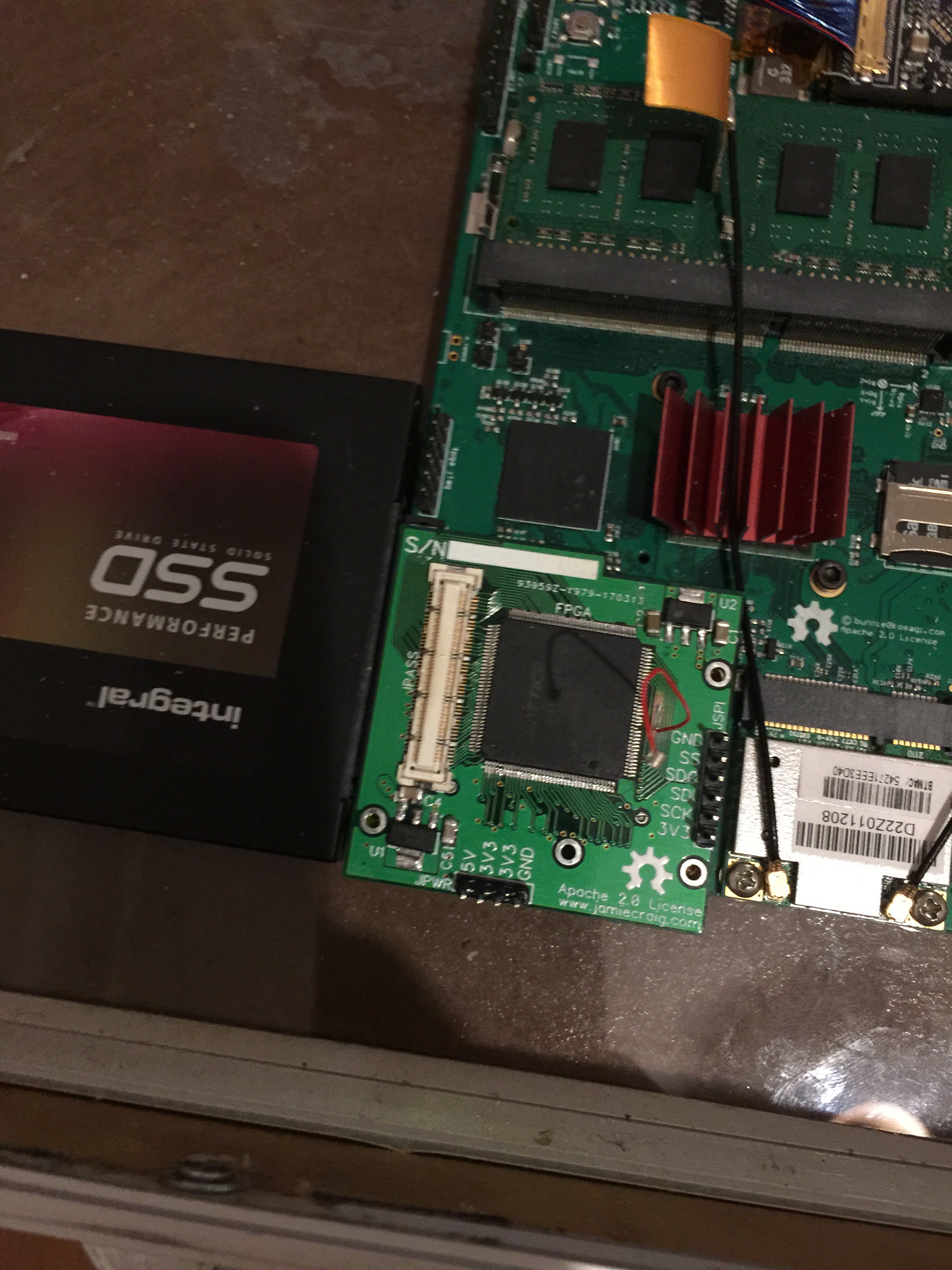
I’ve received the boards for the iCE40 add-on back from DirtyPCBs, and they look good. As far as I can tell, everything seems to be functional, although I’ve got some coding to do before I can tell for certain – in particular, I need to put together a bootloader of some sort to feed the SPI port on the iCE40 with the bitstream.
In the meantime, I’ve put together one of these boards and got it powered up in a spare novena to test, and I’ve quickly thrown together enough Verilog code for the Xilinx to be able to bit-bang SPI to talk to the iCE40.
For anyone following along, the only mistake I’ve noticed on these boards has been the wrong footprint for the upper pass-through connector; the one I’ve used is close enough to fit, but there’s some definite overhang on the pins over the pads, and it’d be wise to redo that part if you’re considering making one of these boards. I’d also recommend using the taller version of the lower connector, as I found the board sits slightly high at one side as a result of resting on the SATA connector. It’s flat enough to still make good contact, however, so if you only have the shorter connectors, you should be OK.
Here’s the board sitting in place in the novena (with a patch wire onto the reset pin during bringup):
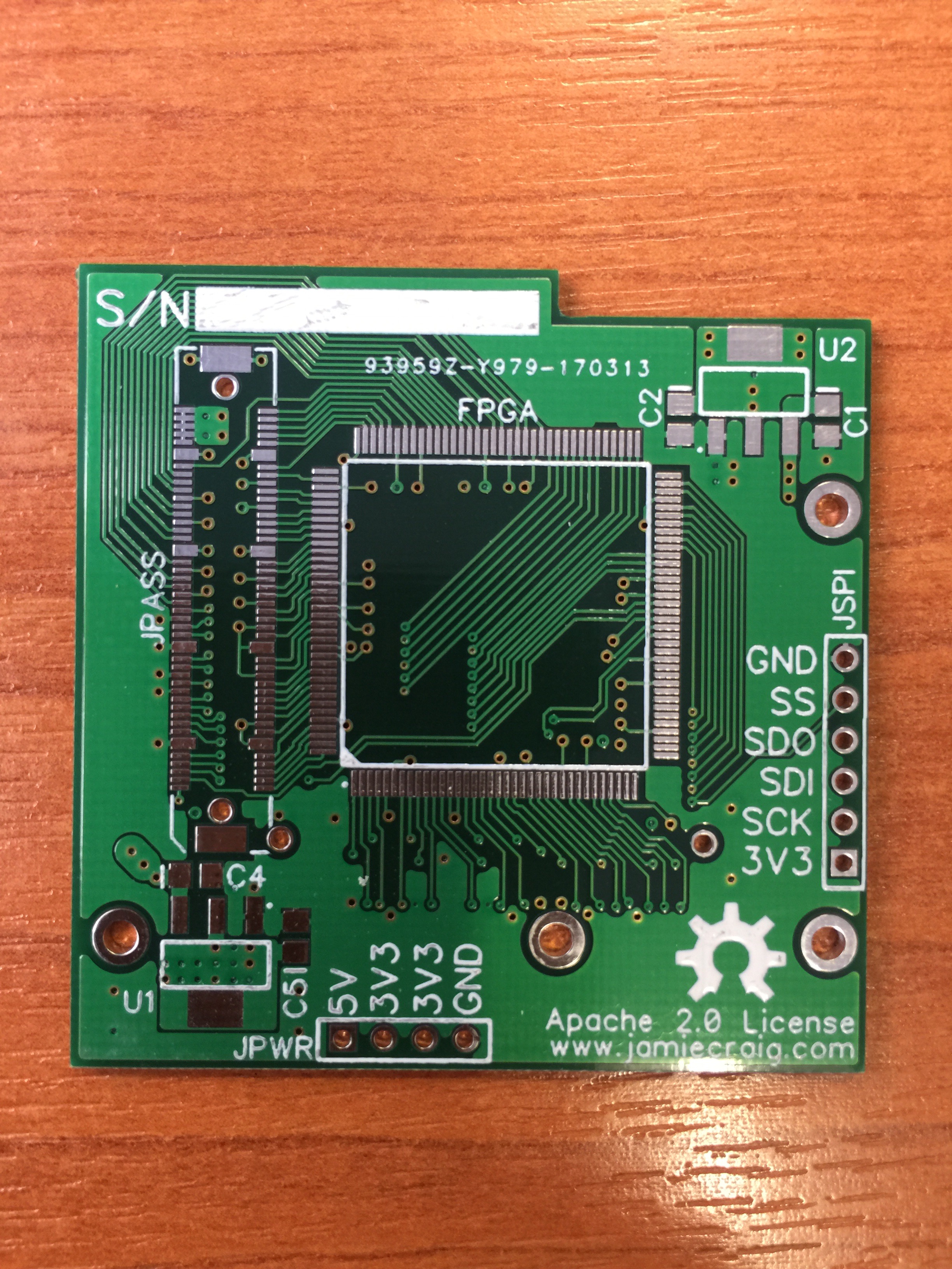
I’ve been working on an add-on board for the Novena open-source laptop, which provides an iCE40HX4K FPGA on a mezzanine board designed to fit in between the Novena and any add-on boards.
The reason this is useful is that Clifford Wolf’sicestorm project provides a fully open-source FPGA toolchain for the iCE40 that can run locally on the Novena, thereby removing the need for an x86 desktop machine when playing with FPGA projects. The Xilinx FPGA will act as a bus bridge between the iCE40 and the Novena, and (hopefully) provide access to RAM too, using a fixed, shared, FPGA design.
The board is intended to sit in the same location as the normal GPBB board would in a Novena laptop, and to provide a rotated FPGA header for the GPBB or other add-on boards to connect to, positioned such that it will sit above the SSD. This isn’t ideal, but the Novena layout is very tight for space around the FPGA connector, so it’s the best way I could fit in space for a whole second board.
At this point, I’ve drawn up a PCB design for the board, and I’ve ordered the first batch from dirtypcbs.com to try out. If anyone’s curious to look at the schematics or board, they’re available here in DipTrace format. Everything’s under the Apache 2.0 license, to match the Novena itself.
I needed to extract the SMB password associated with some address book entries on our Kyocera printers today (Kyocera 4550i’s, specifically) because we’d lost the original password for an account they were using, and we needed to recover it without having to reconfigure every printer in the company. No problem, thinks I, I’ll use KMNet Viewer to dump out the address book to XML from the printer, and just read out the password in the XML.
No such luck. The password’s encrypted in the XML file.
Fortunately, with a little patience and RedGate’s brilliant .NET reflector, I managed to find where the encryption happens, and to extract the relevant keys. The story of how I got this out of the code isn’t particularly exciting, but the final result is that I got the keys to decrypt any password saved in a dump from KMNet viewer. Unfortunately, it’s a fixed key used every time, so you can’t even set your own password to protect your address book dumps – it’s only enough to deter casual snoopers. Not an impressive level of security.
Anyway, without further ado, the relevant information is:-
Passwords are encrypted with DES, in CBC mode, using a key of 41F4A305F38B468F, and an IV of 01820D0B383ECB7C. These are derived from a few variations on the theme of Kyocera’s name via RFC2898; rather than reproduce the original values here, I’ve just included the resulting keys. I found http://des.online-domain-tools.com/ worked fine with these values if you want a quick and dirty online DES decryptor to let you read your address book files.