
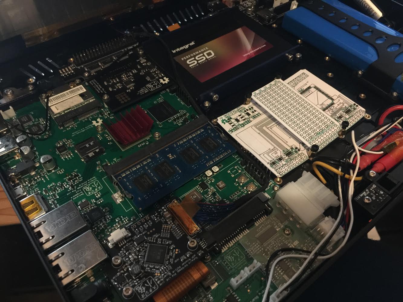
One of the very few complaints I have with the Novena laptop relates to the positioning of the FPGA header on the board. The header is next to an edge of the case, which is important for devices that need external I/O headers, but unfortunately it’s nowhere near the Novena’s Peek array, and therefore hard to combine with internal add-ons. (It’s also a bit close to the CPU heatsink and wireless cards, so you can’t easily use large boards on the FPGA header).
To work around that somewhat, and to try and address some wish-list features I’d have liked on the general-purpose breakout board on the Novena, I’ve been toying with the idea of a bus breakout of sorts, designed to sit in the Peek array, and provide a few buffered I/O slots. Ideally, we want an iCE40 FPGA in there too, to make it easier to build custom FPGA code directly on the Novena – to build for the Xilinx part needs the proprietary Xilinx tools running on a remote machine.
I’d set myself a few basic requirements before starting designing a board for this;
- Add-on devices can appear memory-mapped into the Novena’s address space – this is one of the unique abilities of the Novena FPGA slot vs. devices plugged in over USB or I2C.
- Add-on devices should be able to be 3V, 5V, or any other reasonable voltage without needing to incorporate level-shifting buffers into the device (so you can, for example, use simple 74-series buffers as GPIO for either voltage, selectably)
- At least two, and preferably more, add-on devices should fit into the Peek array, and be able to be mounted securely.
- 0.1″ pitch headers, only, so that add-ons can be made up on Veroboard or perfboard.
- I2C, parallel data, and SPI should all be supported (at any voltage).
When I mentioned some of the details of what I was planning on IRC, Sean Cross (xobs) noted that he’d been considering building something similar with an iCE40 as a catch-all factory test device. I realised that nothing about Pi connectivity fundamentally clashes with the Novena requirements, so I’ve been experimenting with board layouts to try and accommodate both. For the raspberry pi, the main way to talk to the device will be over the SPI port, with both chip selects on the Pi connected up and usable. The same SPI interface allows both reprogramming the FPGA and communicating with it after setup (using two different CS pins). For the Novena, the same approach can be taken, using the SPI port brought out to the front panel board. It’s also possible to use some of the GPBB pins as another SPI port. In both cases the Xilinx FPGA can mediate and present whatever’s attached to the iCE40 as a memory-mapped device. Several extra pins are connected to allow QSPI, UART, and I2C interfaces between the host computer and the iCE40. Of course, since the Pi connector’s pins all go into the iCE40 FPGA, there’s no real requirement that the protocol spoken is SPI at all!
My current work-in-progress is based on a board that fits in a 90mm x 60mm region of the peek array, as shown below, and provides three slots on 30mm spacing. To allow add-on boards as much room adjacent to each other as possible, and a secure mounting directly to the peek array, the boards have notched corners, and a single screw in each corner (which may be shared with the adjacent board) secures them.
My current proposed pin-out for each slot includes a reference voltage pin sandwiched between a 5V pin and a 3.3V pin; this allows a simple jumper to be used to select a suitable voltage, or an external regulator can be used to feed some other reference into the reference pin. Each slot has I2C, SPI, a simple 8-bit bus, and an interrupt pin to allow it to signal for attention.
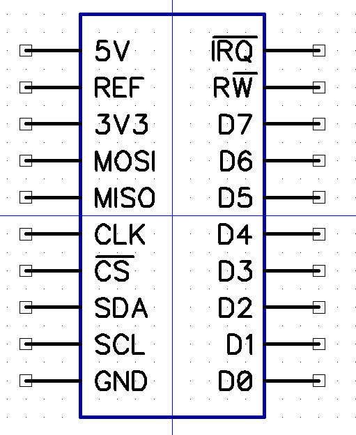
The 8 bit data pins are connected to a bidirectional (switched) level shifter, which can therefore be used for QSPI as well as for a normal 8 bit bus. The other pins are wired to single-direction level shifters as appropriate for the signal role.
As a first “will this even fit” test, I’ve dropped all the key components onto a PCB layout and run the DipTrace autorouter against it; this succeeds even on a 2 layer board, so this design looks achievable. I’d love to hear any feedback on the idea; you can reach me as MadHacker on #kosagi at irc.oftc.net, at the obvious email address, or you can leave a comment below.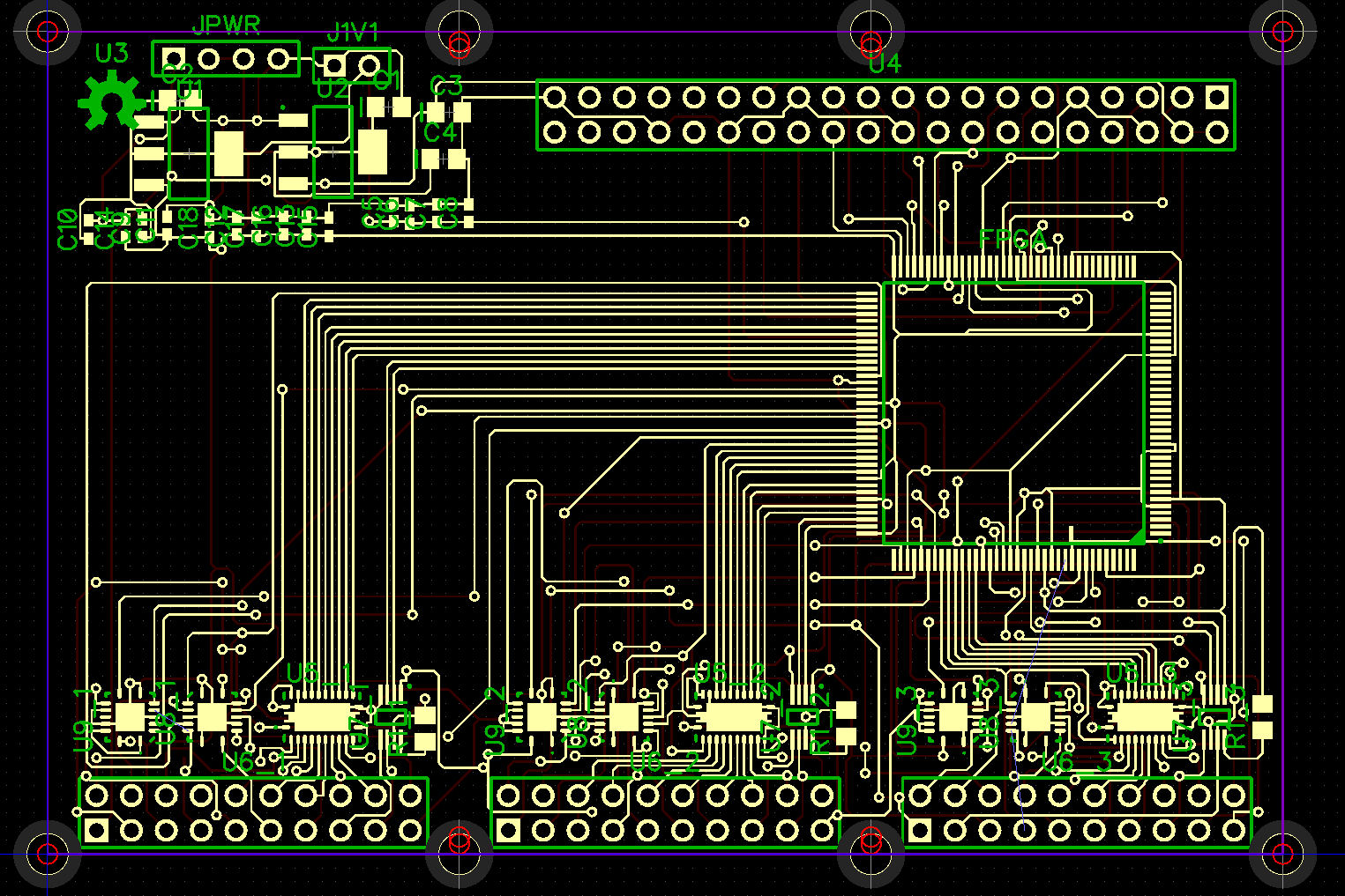
For the 8 -bit I/O bus, I suggest to have a CE and/or CLK/STB pin, so the connected hardware knows when data is valid. You can sacrifice the SPI interface and use that CS and CLK for that (and repurpose MOSI/MISO as an A0 and A1), after all it is programmable :).
The intention was to share them, rather than sacrifice them as such. I’m expecting each device to be using one of these buses, not all three, really (although I2C is there no matter what, so it’s pretty negotiable for that one – I2C ID?).
It’s not obvious from the text where does the Raspberry Pi come in. I suppose xobs’ plan was an add-on ICE board for the Pi?
Yep, pretty much. xobs wanted a board for the pi; I wanted a board for the novena, and the “output” halves looked the same anyway.
The 40-pin connector on the board is wired for the Pi, but I could break out the Novena FPGA connector to the same pinout, or just use a few jumpers to the front panel SPI pins, and support both platforms. A proper breakout board for the Novena FPGA header would allow a bit more bandwidth, since more than just the SPI pins can be wired up to the iCE40 – there’s plenty spare pins in that bank.